|
Research Ideas and Outcomes : Grant Proposal
|
|
Corresponding author: Toma Susi (toma.susi@iki.fi)
Received: 10 Dec 2015 | Published: 17 Dec 2015
© 2016 Toma Susi.
This is an open access article distributed under the terms of the Creative Commons Attribution License (CC BY 4.0), which permits unrestricted use, distribution, and reproduction in any medium, provided the original author and source are credited.
Citation: Susi T (2015) Heteroatom quantum corrals and nanoplasmonics in graphene (HeQuCoG). Research Ideas and Outcomes 1: e7479. doi: 10.3897/rio.1.e7479
|

|
Executive summary
The objective of the Heteroatom quantum corrals and nanoplasmonics in graphene (HeQuCoG) project is to create atomically precise structures made of silicon and phosphorus atoms embedded in the lattice of graphene. This will be achieved by combining proven modeling techniques with sample fabrication via carefully controlled ion implantation, and subsequent manipulation in an atomic resolution scanning transmission electron microscope (STEM). The structures will be computationally designed for interesting nanoplasmonic enhancement and quantum confinement properties, and characterized by electron energy loss spectroscopy mapping in the STEM. The expected outcome is a systematic demonstration of truly atomic-level material design and the creation of freestanding “quantum corral” structures for the first time.
The controlled manipulation of matter on the atomic scale has been a long-standing dream of nanotechnology. Pioneering directions towards have already been explored, chiefly with the help of scanning tunneling microscopy. However, compared to the manipulation of surface atoms, graphene heteroatoms have the advantage of being stable at room temperature and even if the sample is taken out of the instrument. Furthermore, the coupling of light to nanostructures via plasmon resonances is an intensively pursued and promising research field, which is awaiting breakthroughs in material design before the field can live up to its expected potential.
Keywords
atomic manipulation, scanning transmission electron microscopy, electron energy loss spectroscopy, density functional theory, ion implantation
Introduction
This grant proposal is based on the fundamental finding that a relatively low-energy electron beam in an atomic resolution scanning transmission electron microscope can be used to move silicon atoms embedded in the graphene lattice as heteroatoms (see this blog post for a detailed description, and Physical Review Letters for the article). To pursue these findings further, Dr. Susi devised a research plan that combines sample preparation via ion implantation with extensive modeling and electron microscopy experiments. The proposal was funded by the Austrian Science Fund (FWF) in July 2015, with the three-year project starting in September 2015.
Only very few changes were made to the original project plan before submitting it to RIO. These were the removal of the personal contact information of Dr. Susi (for privacy reasons), of the full publication list (for brevity), and of the detailed budget breakdown. The latter was, perhaps surprisingly, the only concern raised by those colleagues consulted on the idea of publishing the proposal. Many expressed their heartfelt support, alongside representatives from the funder and the university. Furthermore, the permission to publish the reports of the original reviewers was requested and gratefully received.
Figure copyrights presented an additional challenge. RIO uses CC BY 4.0 licensing for its machine-readable content, so the usual practice of obtaining RightsLink permissions for reproducing the five literature figures used in the proposal was not satisfactory. Thus, the extra effort to ask the authors for original, non-copyrighted versions of the required figures was undertaken. Thankfully, in this particular instance, all the authors were willing to do this and the proposal could be published in its original form.
1. Scientific aspects
1.1 Aims
The aim of this project is to create atomically precise structures consisting of silicon and phosphorus atoms embedded in the lattice of graphene (called heteroatom in this context). This will be achieved by combining proven modeling techniques with sample fabrication via carefully controlled ion implantation, and subsequent manipulation by atomic resolution scanning transmission electron microscopy (STEM).
The experiments are based on the recent discovery that electron impacts result in the direction-controlled motion of Si atoms in graphene (
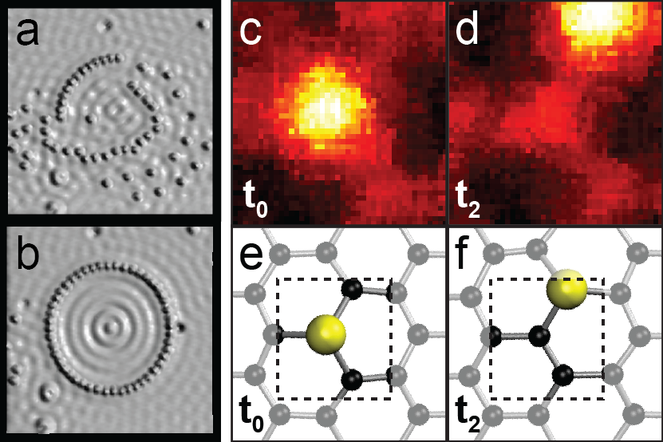
a,b) Scanning tunneling microscopy (STM) images of a Cu(111) surface with iron atoms being assembled (a) into a circular quantum corral structure (b) (
Work towards this aim is divided into three objectives, corresponding to the planned work packages. The first objective is to combine ion implantation simulations with sample preparation and characterization to fabricate the best possible monolayer samples with a sufficient density of substituting heteroatoms. The second objective is to use computational structure screening to identify interesting heteroatom configurations and fabricate them in the microscope. Finally, the third objective completes the aims of the project by modeling and then measuring the electronic response of the created structures via EELS mapping in the STEM.
Physical background
Light absorption can be enhanced in metallic nanostructures by exciting localized surface plasmon modes, producing an antenna effect (
On the other hand, electrons confined to regions with dimensions of the same magnitude as their de Broglie wavelength will be forced to occupy a discrete spectrum. This effect is responsible for the many interesting properties of low-dimensional materials, such as graphene. However, electron confinement can also be purposefully engineered, of which so-called quantum corrals are the most famous example. In a series of pioneering experiments in the early 90’s, researchers at IBM created such structures by painstakingly moving iron atoms one at a time on a copper surface with the tip of a scanning tunneling microscope (
The key tool for manipulating atoms in this project is scanning transmission electron microscopy (STEM), where a very narrow electron beam is scanned in a raster over the sample. With modern aberration-corrected electron optics, resolutions below 0.5 Å can be achieved (
Although electron microscopy is similar to optical microscopy in principle, the fact that electrons carry significant momentum is a crucial difference. Energy transfer from an impinging electron to target nuclei occurs at the zepto (10−21) second time scale, and can thus be described as elastic knock-on collisions between the electrons and the nuclei. Usually this results in unwanted knock-on damage that causes defects, which is in turn mitigated by using lower voltages and limiting the irradiation dose.
Enabling work
The method for moving heteroatoms in the graphene lattice depends on intentionally directing an intense irradiation dose onto a single C atom, which then “jumps” over the bond with the dopant (
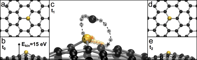
Snapshots of a simulated 150 fs trajectory of a C atom that has received 15 eV of kinetic energy from an energetic electron, based on a density functional theory molecular dynamics (
Based on the DFT simulations conducted by the applicant (
In
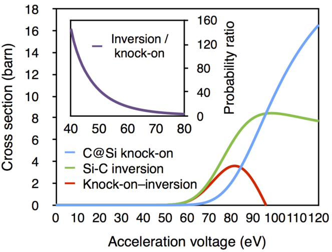
Interaction cross sections for relevant electron-beam induced processes at silicon dopant sites based on DFT calculations conducted previously by the principal investigator (
Innovative aspects
Although quantum corrals are one of the most iconic structures of nanoscience, they only address surface electron states, whereas corresponding freestanding structures have never been made. Further, STM-created structures are not stable in room temperature, which is not an issue for in-lattice structures. And since the crystal structure of graphene results in the carriers having pseudospin, allocating heteroatom to either one or both of the sublattices will likely result in interestingly varying effects.
Although plasmonic enhancement on single Si atoms has been discovered (
Thus, the HeQuCoG project systematically addresses the entire process from sample preparation, to implantation simulations and experiments, to controlled manipulation, and EELS simulations and measurements.
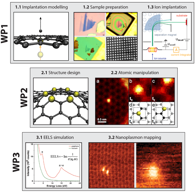
A pictorial illustration of the HeQuCoG project plan, divided into three work packages (WPs, see Section 1.2). The numbered tasks (1.1 to 3.2) are explained in detail in the Methods section below, and citations for images from the literature are given in brackets. Panel captions: 1.1) The implantation of silicon (yellow sphere) into the graphene lattice (black spheres) is simulated via molecular dynamics modeling, yielding optimal ion energies. 1.2) High-quality graphene samples are prepared on Quantifoil TEM grids either from graphene flakes exfoliated onto Si/SiO2 and transferred by immersing the substrate into isopropanol, or from chemically synthesized samples (
Importance to nanoscience
The controlled manipulation of matter on the truly atomic scale has been a long-standing dream of nanotechnology. Compared to the manipulation of surface atoms, structures composed of graphene heteroatoms are likely to prove of greater practical potential than STM-created ones, which have remained a beautiful curiosity. Establishing a platform for reliably designing and defining atomically precise structures with tailored functionality would constitute a major breakthrough in the field.
Furthermore, the coupling of light to nanostructures via plasmon resonances is an intensively pursued and promising research field, with wide-ranging potential applications. However, the losses that inevitably occur in metals severely limit which functionalities are currently feasible (
Finally, it is noteworthy that although ion implantation of silicon forms the basis of modern semiconductor technology, the implantation of heteroatoms into graphene has so far been hardly explored. Any advances in this, or in the preparation of high quality samples, will be of great interest to a large community.
1.2 Methods
Modeling heteroatom implantation (WP1.1)
A computational method for predicting the optimal ion energy for implanting nitrogen and boron atoms into graphene was reported by Åhlgren and co-workers (
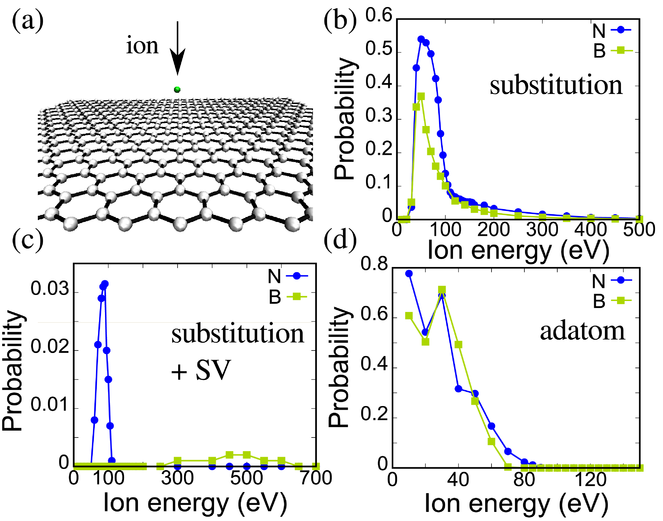
Simulations of N and B implantation into graphene (
In this project, these calculations will first be extended to silicon. For simulating the several hundred thousand required trajectories for the impinging Si ions, a classical potential is required. Several possibilities for modeling the C-C and C-Si interactions exist in the literature, conveniently available in the Atomistica software package (
Graphene sample preparation (WP1.2)
High-quality graphene (either chemically synthesized or exfoliated) will be deposited onto TEM grids with Quantifoil coating (
Ion implantation experiments (WP1.3)
A modest number of defects from high-energy ions would not be an issue for the subsequent stages due to the self-healing nature of graphene vacancies (
The ion implantation experiments (
Computational structure design (WP2.1)
Using a combination of DFT implemented in the real-space, grid-based projector augmented code GPAW (
Prospective structures include linear chains of heteroatoms, gratings consisting of several adjacent rows, and circular, hexagonal or square quantum corrals (i.e., graphene areas delineated by Si or P atoms, see
Atomically precise manipulation of heteroatoms in the STEM (WP2.2)
Two factors determine the optimal voltage for controlled manipulation: knock-on damage should be minimized, but bond inversions should occur sufficiently often. Based on the cross sections in Section 1.1 and the fact that the average time between jumps when irradiating just the Si atom and its three neighbors at 60 kV was around 14 seconds (
The atomic manipulation will be performed with the Vienna UltraSTEM100 by first identifying a clean area of monolayer graphene, and then mapping the number and distribution of heteroatoms in that area using Z-contrast imaging (
Each atom will then be moved one by one to its desired position by directing the electron beam onto the carbon atom into whose place a particular heteroatom must move, and irradiating the spot until the scattered intensity measured at the high angle annular dark field detector increases to indicate that a heavier atom has moved to the beam position. Then the overall structure will again be imaged to confirm the success of the step, and the next move selected in an iterative procedure.
Simulation of the electronic response (WP3.1)
Where computationally feasible, the electronic and plasmonic properties of the structures will be computed in Vienna to give guidance for the measurements. In the GPAW code, the dielectric response can be calculated in the linear regime and the random phase approximation, giving the electron energy loss spectrum from the inverse of the imaginary part of the dielectric function. This approach has been shown to give a good description of the plasmon modes in graphite (
In the experimental setup, low-loss EELS originates from the collective excitations of the electronic system by probe electrons with high momenta perpendicular to the graphene plane. Although some in-plane momentum transfer does occur, for 60 keV electrons losing less than 25 eV, over 90% of the intensity is due to electrons scattered to angles smaller than 1 mrad (
Nanoplasmon mapping (WP3.2)
The nanoplasmonic response of all the created heteroatom configurations will be spatially mapped by measuring the electron energy loss spectrum of the π+σ plasmon found around 15 eV (
The few most promising structures will be investigated with the next generation Nion HERMES (high energy resolution monochromated EELS-STEM) instrument that has just been installed under the supervision of Dr. Quentin Ramasse in the SuperSTEM Laboratory in Daresbury, UK. The electron monochromator included in this literally unique instrument gives unprecedented energy resolution, allowing low energy excitations – even phonons (
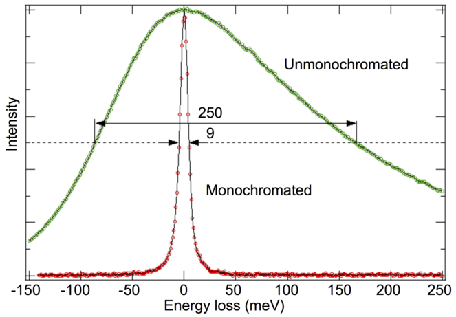
The Nion HERMES can achieve a 9 meV wide (full-width at half-maximum, FWHM) zero loss peak (ZLP), much smaller than the energy distribution of even the best unmonochromated beam produced by the cold field emission electron gun of a cutting-edge UltraSTEM100 microscope. This makes it possible to not only measure very low energy excitations such as phonons (
1.3 Work and time plan
The HeQuCoG project work plan will proceed in the order given in the previous section and in
While the ion implantation experiments are underway, the second Work Package (WP2) will start with the computational design of heteroatom structures, of which at least several dozen different configurations will be explored (Task 2.1). When the implanted samples are ready, the controlled manipulation experiments will start (Task 2.2). These are expected to constitute the most labor-intensive part of the project, and have accordingly been allocated the most time.
While the manipulation experiments are ongoing, the electronic response of selected structures from Task 2.1 will be simulated (Task 3.1). This step will take advantage of research visits to the theoretical spectroscopy group of Prof. Angel Rubio in San Sebastian, Spain. Starting concurrently with the controlled manipulation experiments, the first EELS maps will be collected for WP3 (Task 3.2). In the last stages of Task 3.2, the most interesting structures will be measured in more detail during two extended visits to the SuperSTEM laboratory in Daresbury, UK.
The project time plan is given in
The project work and time plan, divided into three Work Packages (WPs) and 18 two-month periods. Blue bars denote the duration of modeling Tasks (1.1, 2.1 and 3.1), and green bars the duration of experimental Tasks (1.2, 1.3, 2.2, and 3.2).
|
|
Project month |
|
|
|
|
|
|
||||||||||||
|
|
exp. |
|
|
sim. |
|
||||||||||||||
|
|
|
|
|
|
|
||||||||||||||
|
|
Task |
1 |
3 |
5 |
7 |
9 |
11 |
13 |
15 |
17 |
19 |
21 |
23 |
25 |
27 |
29 |
31 |
33 |
35 |
|
WP1 |
1.1 |
|
|
|
|
|
|
|
|
|
|
|
|
|
|
|
|
|
|
|
1.2 |
|
|
|
|
|
|
|
|
|
|
|
|
|
|
|
|
|
|
|
|
1.3 |
|
|
|
|
|
|
|
|
|
|
|
|
|
|
|
|
|
|
|
|
WP2 |
2.1 |
|
|
|
|
|
|
|
|
|
|
|
|
|
|
|
|
|
|
|
2.2 |
|
|
|
|
|
|
|
|
|
|
|
|
|
|
|
|
|
|
|
|
WP3 |
3.1 |
|
|
|
|
|
|
|
|
|
|
|
|
|
|
|
|
|
|
|
3.2 |
|
|
|
|
|
|
|
|
|
|
|
|
|
|
|
|
|
|
|
Risk management
All three Work Packages are designed to contain a balanced mixture of computational and experimental Tasks, which allows progress to be made towards the project goals even if there are unforeseen delays in some of the more challenging experiments. The use of two different heteroatoms, silicon and phosphorus – that are of similar mass and size but of different valence – not only yields complementary information, but gives a degree of robustness to the plan in the unlikely eventuality that there are insurmountable experimental difficulties with one of them.
The EELS measurements in WP3 – particularly using the monochromated Nion HERMES instrument – are of such scientific novelty that even if some of the more ambitious structures envisaged in WP2 prove to be impractical to create, measurements of even a few implanted heteroatom will be scientifically highly interesting. Phosphorus dopants in graphene, in particular, have never been observed by any local probing method. Furthermore, additional techniques such as Raman and X-ray photoelectron spectroscopies of doped samples can and will be used to yield useful complementary information.
1.4 Dissemination
The ongoing results of the HeQuCoG project will be made rapidly available to a broad audience by publishing in high visibility international journals. Direct open access publication via article processing fees (Gold/Hybrid OA) will be strategically utilized for the most important publications, and accepted manuscript versions of all resulting works will be archived in the appropriate repositories (Green OA). All applicable research data and analysis procedures will likewise be made openly accessible either through supplementary information to publications or through data repositories.
Participation and presentations in international conferences will be active. The principal investigator has a proven track record in conference dissemination, with over 20 contributions in the last years, including 11 talks. It is anticipated that the results of the project will be of great interest to the scientific community, and visiting lectures and seminars will be actively pursued whenever possible.
In terms of science outreach, Dr. Susi has a personal blog called Mostly physics (http://mostlyphysics.net), where he explains his topical research for the lay audience. All the main findings of the project will be introduced in this way in as accessible a manner as possible. These efforts will be augmented by an active social media presence (Twitter, Facebook, ResearchGate, LinkedIn, and others), as well as carefully prepared press releases supplemented with multimedia that are sent out through the University of Vienna press office.
1.5 Cooperation arrangements
If the project is funded, the applicant would join the Physics of Nanostructured Materials group (led by Prof. Michael Zehetbauer and Prof. Jannik C. Meyer) at the Faculty of Physics of the University of Vienna. This will enable reliable access to the Vienna Nion UltraSTEM100 instrument capable of atomic resolution TEM/EELS, administered by Prof. Meyer who gives his full support for the project. Dr. Susi has also collaborated and published extensively with Dr. Jani Kotakoski of the same group, who has experience in the simulation of ion implantation into graphene, and whose expertise will be available if needed.
Collaboration with the group of Prof. Paola Ayala at the Faculty of Physics, who is a long-standing colleague of the principal investigator, will enable access to multifrequency Raman and x-ray photoelectron spectroscopy instrumentation that will be used for sample preparation and complementary measurements. The electron energy loss spectroscopy simulations will draw on the expertise of the theoretical spectroscopy group of Prof. Angel Rubio in San Sebastian, Spain. The group is internationally recognized for their leading role in such simulations, and Dr. Susi has made extended visits to the group and already published together with the group EELS expert Dr. Duncan Mowbray.
The ion implantation experiments will be conducted at the University of Göttingen ion beam deposition system in collaboration with the group of Prof. Hans Hofsäss. Although Dr. Susi has not yet published together with him, an introduction was made by a common co-author (Prof. Ursel Bangert) for whom Prof. Hofsäss previously successfully performed ultra low energy (< 25 eV) ion implantation doping of graphene with B and N heteroatoms (
The fundamental finding underlying the present project plan – the possibility to move silicon atoms with an electron beam – was discovered in collaboration with Prof. Quentin Ramasse, the scientific director the the SuperSTEM Laboratory in Daresbury, UK. The laboratory has just received the first accessible monochromated Nion HERMES instrument in the world, which will allow for dramatically more detailed nanoplasmon measurements and over the entire optical range. Although access to the facility incurs usage costs at a flat daily rate, Prof. Ramasse has offered to match in kind the usage time budgeted in this project by the official participation of the SuperSTEM center.
2. Human resources
2.1 Academic qualifications
The principal investigator (PI) of the project is Dr. Toma Susi, who is originally from Finland and is in August 2015 completing a two-year FWF Lise Meitner fellowship in the group of Prof. Ayala at the Faculty of Physics of the University of Vienna. Due to his uniquely suitable set of skills for the purposes of the research plan, the project will employ him as a senior postdoctoral researcher. In addition, one doctoral student will be hired for the project and co-supervised by the PI and Prof. Meyer.
During his thesis, Dr. Susi was the leading Aalto University researcher in the EU FP6 project BNC Tubes on heterodoped nanotubes (2008-2011). His opponent, Prof. Mauricio Terrones, is one of the pioneering experts in the field, and one of his thesis pre-examiners, Dr. Chris Ewels, is the author of the most cited review on the topic. Based on work performed in international collaborations with experimentalists and theorists, the thesis work “Nitrogen-doped single-walled carbon nanotube thin films” spanned the topic from synthesis mechanism studies to materials synthesis, from spectroscopy and microscopy to thin film film application studies. The dissertation was awarded the highest grade, and awarded as the thesis of the year 2011.
During the course of his 3.5-year PhD and the subsequent two-year postdoc, Dr. Susi published 18 peer-reviewed articles in leading international journals including JACS, Chemistry of Materials, Nano Letters, PhysChemChemPhys, Carbon, and Journal of Physical Chemistry. During the first year of his Lise Meitner fellowship in Vienna, he has been mainly working on calculating core level binding energies for x-ray photoelectron spectroscopy (resulting in several publications and a review article on the topic), and on simulating the effects of electron beam irradiation on doped graphene. He lead the collaboration that resulted in the recent Physical Review Letter (
The PI has experience operating the UltraSTEM100 microscope already during a visit to the Oak Ridge National Laboratory in 2013, and now more extensively in Vienna. A multiple-time co-author and close colleague in Vienna, Dr. Jani Kotakoski, was originally responsible for simulating the ion implantation of N and B into graphene, which will be extended in WP1.1, and has familiarized Dr. Susi with the methodology.
As described above, previous work by the applicant has familiarized him with the relevant electron microscopy and simulation techniques. Combined with his in-depth knowledge on the topic demonstrated by this project plan, this makes him a perfect person to also carry out the project in practice. Furthermore, he already has a proven record of collaboration with most of the key research partners.
2.2 Importance for career development
Despite his young age, the principal investigator has already exhibited strong leadership and management qualities. He was instrumental in helping coordinate the large FP6 STREP project BNC Tubes, from communicating with the consortium partners and managing budgets to compiling all of the project reporting. The Lise Meitner fellowship Dr. Susi received in 2013 demonstrates his willingness to seek the most rewarding research environment and to obtain competitive research funding.
The PI has clearly reached a position of high maturity for his stage of career. The opportunity to lead his personal research project will take him to the next level and prepare him for a position of leadership in the academic sphere. The multidisciplinary nature of the research, as well as the opportunities for high-level experimental and theoretical collaboration at the University of Vienna and abroad would be a firm push forward, propelling him to a position of professional maturity.
Intensive microscopy experiments will deepen the practical skills of the PI at the very highest scientific level. Analysis of the results using the latest rigorous methods and advanced algorithms is another crucial facet of the gained experience. Dr. Susi also has a strong background in physics and a keen interest in density functional theory methods. Simulations of ion implantation and electron energy loss spectra are both novel problems, but which are naturally related to and extend from his pre-existing expertise.
The PI would naturally also be in charge of the dissemination of the project, leading the writing of the resulting publications, continuing his very active participation in international conferences and workshops, and expanding his public outreach activities. The interaction with several world-class research groups in Vienna will allow him to extend his already strong international collaboration network and prepare him for a leading position in the community.
Furthermore, Vienna has proven to be an extremely stimulating and productive research environment for Dr. Susi, and a possibility to continue building on the results obtained during his time there will be extremely valuable. After three further years of leading an ambitious and cutting-edge research project, he will be eminently eligible for starting to apply for more prestigious personal grants and tenure tracks positions either in Austria, or elsewhere in the world.
The doctoral student to be hired will have an excellent opportunity to complete their dissertation in an internationally high level research project under close and intensive supervision. At the same time, co-supervising the student will be vital experience for the the principal investigator on his academic career.
3. Potential additional aspects
3.1 Implications for other branches of science
In the broad conception of the branches of science as being the natural sciences, the formal sciences, and the social sciences, we do not foresee that significant implications beyond the natural sciences would result from the project.
However, considering the vast interest that quantum corrals have generated far outside the specific surface science community where they were discovered, should the project prove successful, it will surely have a chance to contribute significantly to the public understanding of science, and to pushing the limits of what is technologically possible both in the popular imagination and within science. The University of Vienna, and Austrian science in general, would accordingly receive significant positive attention due to the findings.
3.2 Effects with implications beyond specific field
The controlled creation of atomically defined nanostructures and their electron spectroscopy are the main topics of research directly related to this project. Beyond these, the availability of atomically precisely designed structures would undoubtedly have far-reaching implications for many fields of the physical sciences.
To highlight one intriguing possibility: a novel atomic probe microscopy technique uses two specifically designed scanning tunneling microscopy tips that can probe graphene from both sides (
Although very challenging, such measurements of pre-defined atomic structures could be enabled by this project, and would yield unparalleled detailed information on the effect atomically precise heteroatom arrangements have on quantum transport properties, which could then be benchmarked against state-of-the-art transport simulations.
4. Financial aspects
4. Financial aspects
4.1 Information on the research institution
The site of research is the Faculty of Physics at the University of Vienna. It is the oldest university in the German-speaking world – celebrating its 650th anniversary in 2015 – and one of the largest in Central Europe. The university has a strong focus on research, combining fundamental with application-oriented research.
The primary research team with whom the project plan will be implemented in Vienna is the group of internationally recognized microscopy expert Prof. Jannik Meyer. His group administers one of the handful Nion UltraSTEM100 microscopes operating in the world at the current moment. Their instrument is specifically modified for in-situ experiments, such as gas exposure and deposition during observation. The group has also recently received a dual-probe STM setup, which is unique in the world.
Furthermore, Dr. Susi is already an active user of the Vienna Scientific Cluster, which presents ample computational resources to carry out the simulation aspects of the research. Assistance with project management will be available through the group secretary, and technical and IT support through the Faculty of Physics.
4.2 Information on the support requested
The personnel costs of the project consist of a full-time senior postdoc salary for the independent applicant Dr. Toma Susi for the first two years of the project, and half-time for the third year. The principal investigator will personally conduct the computational research tasks, and partly conduct and lead the experimental ones. The funding will allow him to continue his fruitful research in Austria following the completion of his Lise Meitner fellowship, and to apply for supplementary funding from the third year onwards. In addition, the personnel costs cover the salary of a doctoral student (75% time contribution).
Material costs consist of two items vital for the project plan: TEM sample grids (WP 1.2), and materials required for the ion source (WP 1.3). Access to the HERMES microscope in Daresbury for the required 10 days will be financed by a payment from the project budget, and an additional donation in kind from SuperSTEM. Finally, the proposed collaboration requires extended visits to Göttingen in Germany, San Sebastian in Spain, and Daresbury in the UK (six stays of two weeks expected in total).
The total budget for the project (including 5% general costs) is 323 972.25 €
5. Academic CVs and publications
5.1 Dr. Toma Susi
Education
Doctor of Science (Technology), Aalto University, Espoo, Finland (June 2011)
Web
http://www.researcherid.com/rid/C-2989-2009
Main areas of research
Heteroatom doping, graphene, density functional theory simulations, electron beam damage, single-walled carbon nanotubes, x-ray photoelectron spectroscopy
ACADEMIC CAREER
University of Vienna (Austria) since 9/2013
FWF Lise Meitner Fellow, Tailored Hybrid Structures group
Two year fellowship funded by the Austrian Research Funder (FWF) on studying nitrogen- and phosphorus-doped single-walled carbon nanotubes (SWCNTs).
Aalto University School of Science (Finland) 6/2011–8/2013
Postdoctoral researcher, NanoMaterials group
Building on the doctoral thesis work with extensive international collaboration. Wide-ranging responsibility for project reporting and management.
Helsinki University of Technology (Finland) 1/2008–5/2011
Research Scientist, NanoMaterials group
PhD thesis: Nitrogen-doped SWCNTs synthesis with controllable doping. Assisting the coordinator in project reporting and management in the EU FP6 Novel Heteroatomic Boron, Nitrogen and Carbon Nanotubes project.
Helsinki University of Technology (Finland) 1/2007–8/2007
Research assistant, NanoMaterials group
M.Sc. thesis: Single- and multiwalled carbon nanotube CVD synthesis.
Helsinki University of Technology (Finland) 6/2006–12/2006
Research assistant, Surfaces and Interfaces on the Nanoscale group
Bachelor thesis: The effect of iron-carbon interaction on the magnetism of carbon nanotubes.
ACADEMIC RECOGNITION
Academic prizes
- Thesis of the Year award (Assoc. Finnish Engineers and Architects) 2012
- Doctoral thesis awarded highest grade “Pass with distinction” 2011
- Awarded scholarship for a swift completion of the master’s degree 2011
Selected talks in scientific conferences
- International Conference on the Science and Application of Nanotubes 2014
- Heteronanocarb (Barcelona, Spain) 2013 (talk awarded as the “Best oral presentation”)
- A3 Symposium of Emerging Materials (Tohoku, Japan) 2012 (talk awarded as the “Best oral presentation”)
- Towards reality in nanoscale materials (Levi, Finland) 2012
- Nanotube photonics and optoelectronics workshop (Koli, Finland) 2010 (talk awarded as the “Best student oral presentation”)
Reviewer for
Nanotechnology, Physica Scripta, Journal of Physics D (Institute of Physics), Materials Express (American Scientific Publishers)
FUNDING AND PROJECT MANAGEMENT
Personal Funding
- FWF Lise Meitner fellowship 9/2013–8/2015
- Finnish Cultural Foundation mobility grant 3/2013
- Walter Ahlström Foundation mobility grant 4/2013
- Department of Applied Physics funding for finalizing PhD thesis 4/2011
- Finnish Foundation for Technology Promotion personal stipend 5/2011
Project management
- EU FP7 project E-SIGNAGE responsible project manager 2011–2013
- Aalto MIDE program visiting professorship, Yutaka Ohno 2012–2013
- Finnish TEKES project CNT-GROCO 2008–2011
- EU FP6 project BNC Tubes assistant coordinator 2008–2011
Key international cooperation
- Esko Kauppinen (Aalto University, Finland)
- Annick Loiseau (ONERA-CNRS, France)
- Raul Arenal (University of Zaragoza, Spain)
- Christopher Ewels (Institut des Matériaux Nantes, France)
- Duncan Mowbray (University of the Basque Country, Spain)
- Quentin Ramasse (SuperSTEM, UK)
10 most important publications to date
- Susi, T., Kotakoski, J., Kepaptsoglou, D., Mangler, C., Lovejoy, T.C., Krivanek, O.L., Zan, R., Bangert, U., Ayala, P., Meyer, J.C., and Ramasse, Q., Silicon–Carbon Bond Inversions Driven by 60-keV Electrons in Graphene, Phys. Rev. Lett. 113, 115501 (2014, CC-BY). doi:10.1103/PhysRevLett113.115501
- Susi, T., Kotakoski, J., Arenal, R., Kurasch, S., Jiang, H., Skakalova, V., Stephan, O., Krasheninnikov, A.V., Kauppinen, E.I., Kaiser, U., and Meyer, J.C., Atomistic Description of Electron Beam Damage in Nitrogen-Doped Graphene and Single-Walled Carbon Nanotubes, ACS Nano 6, 8837 (2012). doi:10.1021/nn303944f
- Susi, T., Mowbray, D.J., Ljungberg, M.P., and Ayala, P., Calculation of the graphene C 1s core level binding energy, Phys. Rev. B 91, 081401(R) (2015). doi:10.1103/PhysRevB.91.081401.
- Susi, T., Pichler, T., Ayala, P., X-ray photoelectron spectroscopy of graphitic carbon nanomaterials, Beilstein J. Nanotechnol. 6, 177 (2015). doi:10.3762/bjnano.6.17
- Susi, T., Kaskela, A., Zhu, Z., Ayala, P., Arenal, R., Tian, Y., Laiho, P., Mali, J., Nasibulin, A.G., Jiang, H., Lanzani, G., Stephan, O., Laasonen, K., Pichler, T., Loiseau, A., Kauppinen, E.I., Nitrogen-Doped Single-Walled Carbon Nanotube Thin Films Exhibiting Anomalous Sheet Resistances, Chem. Mater. 23, 2201 (2011). doi: 10.1021/cm200111b
- Tison, Y., Lin, H., Lagoute, J., Repain, V., Chacon, C., Girard, Y., Rousset, S., Henrard, L., Zheng, B., Susi, T., Kauppinen, E.I., Ducastelle, F., and Loiseau, A., Identification of Nitrogen Dopants in Single-Walled Carbon Nanotubes by Scanning Tunneling Microscopy, ACS Nano 7, 7219 (2013). doi:10.1021/nn4026146
- Susi, T., Kaukonen, M., Havu, P., Ljungberg, M.P., Ayala, P., and Kauppinen, E.I., Core level binding energies of functionalized and defective graphene, Beilstein J. Nanotechnol. 5, 121 (2014). doi:10.3762/bjnano.5.12
- Ruiz-Soria, G., Susi, T., Sauer, M., Yanagi, K., Pichler, T., Ayala, P., On the bonding environment of phosphorus in purified doped single-walled carbon nanotubes, Carbon 81, 91 (2015). doi:10.1016/j.carbon.2014.09.028
- Susi, T., Lanzani, G., Nasibulin, A.G., Ayala, P., Jiang, T., Bligaard, T., Laasonen, K., and Kauppinen, E.I., Mechanism of the initial stages of nitrogen-doped single-walled carbon nanotube growth, Phys. Chem. Chem. Phys. 13, 11303 (2011). doi: 10.1039/c1cp20454h
- Zhu, Z., Jiang, H., Susi, T., Nasibulin, A., and Kauppinen, E.I., The Use of NH3 to Promote the Growth of Large-Diameter SWCNTs with a Narrow (n,m) Distribution, J. Amer. Chem. Soc. 133, 1224 (2011). doi: 10.1021/ja1087634
Funding program
FWF Stand-alone project.
Hosting institution
University of Vienna, Faculty of Physics, Physics of Nanostructured Materials.
International cooperation
- Prof. Hans Hofsäss (University of Göttingen, Germany)
- Prof. Quentin Ramasse (SuperSTEM Daresbury, UK)
- Prof. Angel Rubio (ETSF, San Sebastian, Spain)
Author contributions
Toma Susi conceived and wrote the proposal. Helpful discussions with Jani Kotakoski, Jannik Meyer, Duncan Mowbray, Angel Rubio, Hans Hofsäss and Quentin Ramasse are gratefully acknowledged.
References
-
Atomistic simulations of the implantation of low-energy boron and nitrogen ions into graphene.Physical Review B83(11):115424. DOI: 10.1103/physrevb.83.115424
-
Dry-cleaning of graphene.Applied Physics Letters104(15):153115. DOI: 10.1063/1.4871997
-
Ion Implantation of Graphene—Toward IC Compatible Technologies.Nano Letters13(10):4902‑4907. DOI: 10.1021/nl402812y
-
How can a particle absorb more than the light incident on it?American Journal of Physics51(4):323. DOI: 10.1119/1.13262
-
Confinement of Electrons to Quantum Corrals on a Metal Surface.Science262(5131):218‑220. DOI: 10.1126/science.262.5131.218
-
Probing from Both Sides: Reshaping the Graphene Landscape via Face-to-Face Dual-Probe Microscopy.Nano Letters13(5):1934‑1940. DOI: 10.1021/nl3042799
-
Electron energy-loss spectroscopy in the TEM.Reports on Progress in Physics72(1):016502. DOI: 10.1088/0034-4885/72/1/016502
-
Analytical potential for atomistic simulations of silicon, carbon, and silicon carbide.Physical Review B71(3):035211. DOI: 10.1103/physrevb.71.035211
-
Raman Spectrum of Graphene and Graphene Layers.Physical Review Letters97(18):187401. DOI: 10.1103/physrevlett.97.187401
-
Electron microscopy image enhanced.Nature392(6678):768‑769. DOI: 10.1038/33823
-
Doping and growth of diamond-like carbon films by ion beam deposition.Diamond and Related Materials3:137‑142. DOI: 10.1016/0925-9635(94)90045-0
-
How to deal with the loss in plasmonics and metamaterials.Nature Nanotechnology10(1):2‑6. DOI: 10.1038/nnano.2014.310
-
Atom-by-atom structural and chemical analysis by annular dark-field electron microscopy.Nature464(7288):571‑574. DOI: 10.1038/nature08879
-
Vibrational spectroscopy in the electron microscope.Nature514(7521):209‑212. DOI: 10.1038/nature13870
-
Anisotropy and Interplane Interactions in the Dielectric Response of Graphite.Physical Review Letters89(7):076402. DOI: 10.1103/physrevlett.89.076402
-
The Coulomb Scattering of Relativistic Electrons by Nuclei.Physical Review74(12):1759‑1763. DOI: 10.1103/physrev.74.1759
-
Hydrocarbon lithography on graphene membranes.Applied Physics Letters92(12):123110. DOI: 10.1063/1.2901147
-
Real-space grid implementation of the projector augmented wave method.Physical Review B71(3):035109. DOI: 10.1103/physrevb.71.035109
-
Theoretical electron energy loss spectroscopy of isolated graphene.physica status solidi (b)251(12):2509‑2514. DOI: 10.1002/pssb.201451174
-
Screened empirical bond-order potentials for Si-C.Physical Review B87(20):205410. DOI: 10.1103/physrevb.87.205410
-
Ion implanter schematic. Licensed under CC BY-SA 3.0 via Wikimedia Commons. http://commons.wikimedia.org/wiki/File:Ion_implanter_schematic.png. Accession date: 2015 1 26.
-
Theoretical Analysis of a Dual-Probe Scanning Tunneling Microscope Setup on Graphene.Physical Review Letters112(9):096801. DOI: 10.1103/physrevlett.112.096801
-
Silicon–Carbon Bond Inversions Driven by 60-keV Electrons in Graphene.Physical Review Letters113(11):115501. DOI: 10.1103/physrevlett.113.115501
-
Investigation of the effect of low energy ion beam irradiation on mono-layer graphene.AIP Advances3(7):072120. DOI: 10.1063/1.4816715
-
Graphene Reknits Its Holes.Nano Letters12(8):3936‑3940. DOI: 10.1021/nl300985q
-
Atomically localized plasmon enhancement in monolayer graphene.Nature Nanotechnology7(3):161‑165. DOI: 10.1038/nnano.2011.252
Supplementary material
The attachment contains the original reports given to the FWF by the reviewers of the grant application, published here with their permission.
Reviewer A, Sokrates T. Pantelides from Vanderbilt University in the USA, consented to revealing their name alongside the report. Reviewer B wished to remain anonymous.
Download file (142.54 kb)